
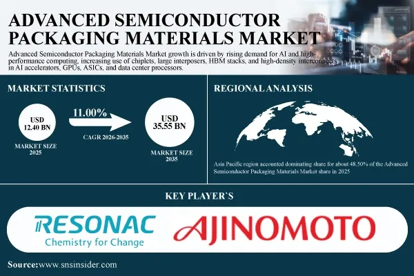
SNS Insider Estimates, the Advanced Semiconductor Packaging Materials Market is projected to reach USD 35.55 billion by 2035, growing at a 11.00% CAGR, while the U.S. market is projected to reach USD 9.92 billion, advancing at a 13.90% CAGR, as AI accelerators, HBM, chiplets and advanced packaging investments accelerate demand for high-performance materials.
Austin, Sept. 25, 2026 (GLOBE NEWSWIRE) -- The global Advanced Semiconductor Packaging Materials Market was valued at USD 12.40 billion in 2025 and is projected to reach USD 35.55 billion by 2035, expanding at a CAGR of 11.00% during 2026–2035. Demand is being supported by AI accelerators, GPUs, custom AI ASICs, data center processors, HBM stacks and increasingly complex chiplet architectures requiring specialized substrates, dielectrics, underfills, encapsulants, thermal interface materials and high-density interconnect solutions.
The U.S. Advanced Semiconductor Packaging Materials Market was valued at approximately USD 2.70 billion in 2025 and is projected to reach approximately USD 9.92 billion by 2035, growing at a CAGR of 13.90% during 2026–2035. Growth is being supported by domestic investment in advanced packaging, AI accelerator demand, semiconductor supply-chain incentives and continued development of glass-core substrates, 2.5D/3D packaging and heterogeneous integration technologies.
Get a Sample Report of Advanced Semiconductor Packaging Materials Market Forecast @ https://www.snsinsider.com/sample-request/11150
The Europe Advanced Semiconductor Packaging Materials Market was valued at approximately USD 2.36 Billion in 2025 and is projected to reach approximately USD 6.34 Billion by 2035, growing at a CAGR of approximately 10.30% during 2026–2035. Growth is driven by the semiconductor materials and equipment industry in Germany, the demand for automotive and industrial electronics and investments in advanced packaging, heterogeneous integration, and reliable semiconductors in Europe, particularly Germany, France and the Netherlands.
Why this Market is Gaining Attention in 2026
AI Accelerators Are Raising Advanced Packaging Material Requirements
Complex packaging designs which integrate chiplet structures, HBM stacks and large interposers are used in AI processors. Such designs use special substrates, dielectrics, underfills, encapsulants and thermal interface materials.
As AI training and inference infrastructure scales, packaging materials are becoming increasingly important to overall semiconductor performance, reliability and thermal management.
HBM is Creating a Parallel Opportunity for Materials Suppliers
Successive generations of high-bandwidth memory require increasingly fine-pitch interconnects, improved bonding materials and packaging systems capable of supporting taller memory stacks and greater interface bandwidth.
This creates substantial opportunities for suppliers developing hybrid bonding materials, advanced interposers, thermal-management solutions and high-reliability underfill technologies.
Glass Substrates and Hybrid Bonding Expand the Market Opportunity
The trend towards glass core substrates provides an opening for materials that can enable larger packages and be dimensionally stable and resistant to warpage.
On the other hand, hybrid bonding is creating a need for advanced copper interconnect and dielectric materials that can provide sub-micron pitch and interconnect density in next-generation HBM and logic devices.
For Analyst-Curated Insights Customized to Your Business, Connect Now @ https://www.snsinsider.com/request-analyst/11150
Commercial Findings from the Advanced Semiconductor Packaging Materials Market
By Material Type, Advanced Packaging Substrates Dominated and Interconnect Materials are the Fastest Growing: In 2025, Advanced Packaging Substrates segment is expected to hold around 34.50% of the market, owing to their significance in all advanced packaging applications and rising usage of glass and next-gen substrate technology. Interconnect Materials are anticipated to grow at the highest CAGR of around 16.80%, owing to hybrid bonding and growing demand for fine pitch copper interconnections.
By Packaging Technology, 2.5D Interposer-Based Packaging Dominated and Hybrid Bonding is the Fastest Growing: 2.5D Interposer-based Packaging accounted for about 28.50% of the market share in 2025 due to wide-scale adoption in AI accelerators and HBM technologies. Hybrid bonding technology is expected to show the highest CAGR growth of about 18.20% due to lower interconnect pitch sizes and thermal resistance.
By Application, AI & High-Performance Computing Dominated and High-Bandwidth Memory is the Fastest Growing: AI & High Performance Computing together had an approximate market share of 32.50% in 2025 owing to the demand coming from GPUs, AI accelerators, ASICs, and data center processors. High Bandwidth Memory is expected to have the highest CAGR of 17.60% owing to increased stack height and bandwidth by memory companies.
By End User, Semiconductor Foundries Dominated and Memory Manufacturers are the Fastest Growing: Semiconductor Foundries constituted nearly 38.50% share of the market in 2025, backed by significant capital expenditure on advanced packaging and increasing demands from AI and HPC customers. The growth rate of Memory Manufacturers is expected to be the highest at 15.80%, on account of increasing consumption of interposer, dielectric, underfill, encapsulant and thermal material with each successive HBM generation.
Regional Advanced Packaging Investment is Reshaping Market Demand: The share of Asia Pacific was approximately 48.50% in the global market in 2025 owing to the presence of key foundries, OSATs, HBM manufacturers, and advanced packaging manufacturing capabilities. North America is projected to grow strongly due to rising investments in the advanced packaging manufacturing industry and AI semiconductor manufacturing industry.
Purchase Single User PDF of Advanced Semiconductor Packaging Materials Market Report @ https://www.snsinsider.com/checkout/11150
Who Should be Watching the Advanced Semiconductor Packaging Materials Market?
The market is increasingly relevant across the broader semiconductor ecosystem, including:
Semiconductor foundries → memory manufacturers → OSAT companies → substrate suppliers → materials companies → AI chip designers → advanced packaging providers → data center semiconductor companies → electronics manufacturers
For materials suppliers, competitive positioning increasingly depends on dielectric performance, thermal conductivity, low warpage, fine-pitch compatibility, bonding reliability and qualification for next-generation 2.5D, 3D and HBM architectures.
Advanced Packaging Materials and Heterogeneous Integration Shape the 2026 Market
As AI and HBM architectures increase package complexity, materials companies are expanding specialized semiconductor packaging portfolios.
- In 2026, Resonac Holdings expanded its semiconductor and IC packaging materials capabilities across Asia Pacific and North America, advancing copper-clad laminates, package substrates and encapsulation materials.
- In 2026, Shin-Etsu Chemical expanded production of photoresists, encapsulants and silicon-based packaging materials as investment in chiplet and advanced packaging architectures increased.
Market Challenge: Scaling Advanced Packaging Materials Without Increasing Cost and Qualification Complexity
Advanced substrates, dielectrics and bonding materials carry higher research and manufacturing costs than conventional packaging materials. Commercial adoption also requires extensive qualification to verify reliability and compatibility with semiconductor manufacturing processes.
Emerging technologies such as glass-core substrates remain constrained by limited manufacturing capacity, while integration with existing production infrastructure creates additional technical challenges. As a result, suppliers are increasingly competing on reliability, manufacturability, qualification speed and compatibility with next-generation packaging processes.
Rising Demand for Advanced Semiconductor Packaging Materials Market Data, Our Full Report Trend Analysis @ https://www.snsinsider.com/reports/advanced-semiconductor-packaging-materials-market-11150
Key Competitors in the Market
Companies covered in the Advanced Semiconductor Packaging Materials Market research include Henkel AG & Co. KGaA, Resonac Holdings Corporation, Shin-Etsu Chemical Co., Ltd., DuPont de Nemours, Inc., Dow Inc., Samsung Electro-Mechanics Co., Ltd., Ajinomoto Co., Inc., NAMICS Corporation, Sumitomo Bakelite Co., Ltd., Kanto Chemical Co., Inc., Fujifilm Corporation, Merck KGaA, Indium Corporation, MacDermid Alpha Electronics Solutions, ASE Technology Holding Co., Ltd., Taiwan Semiconductor Manufacturing Company, Amkor Technology, Inc., JCET Group Co., Ltd., Ibiden Co., Ltd., and Unimicron Technology Corp.
About SNS Insider
SNS Insider is one of the leading market research and consulting agencies that dominates the market research industry globally. Our company's aim is to give clients the knowledge they require in order to function in changing circumstances. In order to give you current, accurate market data, consumer insights, and opinions so that you can make decisions with confidence, we employ a variety of techniques, including surveys, video talks, and focus groups around the world.
CONTACT: Rohan Jadhav - Principal Consultant
Phone: +1-315 636 4242 (US) | +44- 20 3290 5010 (UK)

Comments (0)
Login to join the conversation
Login / RegisterNo comments yet. Be the first to comment!